
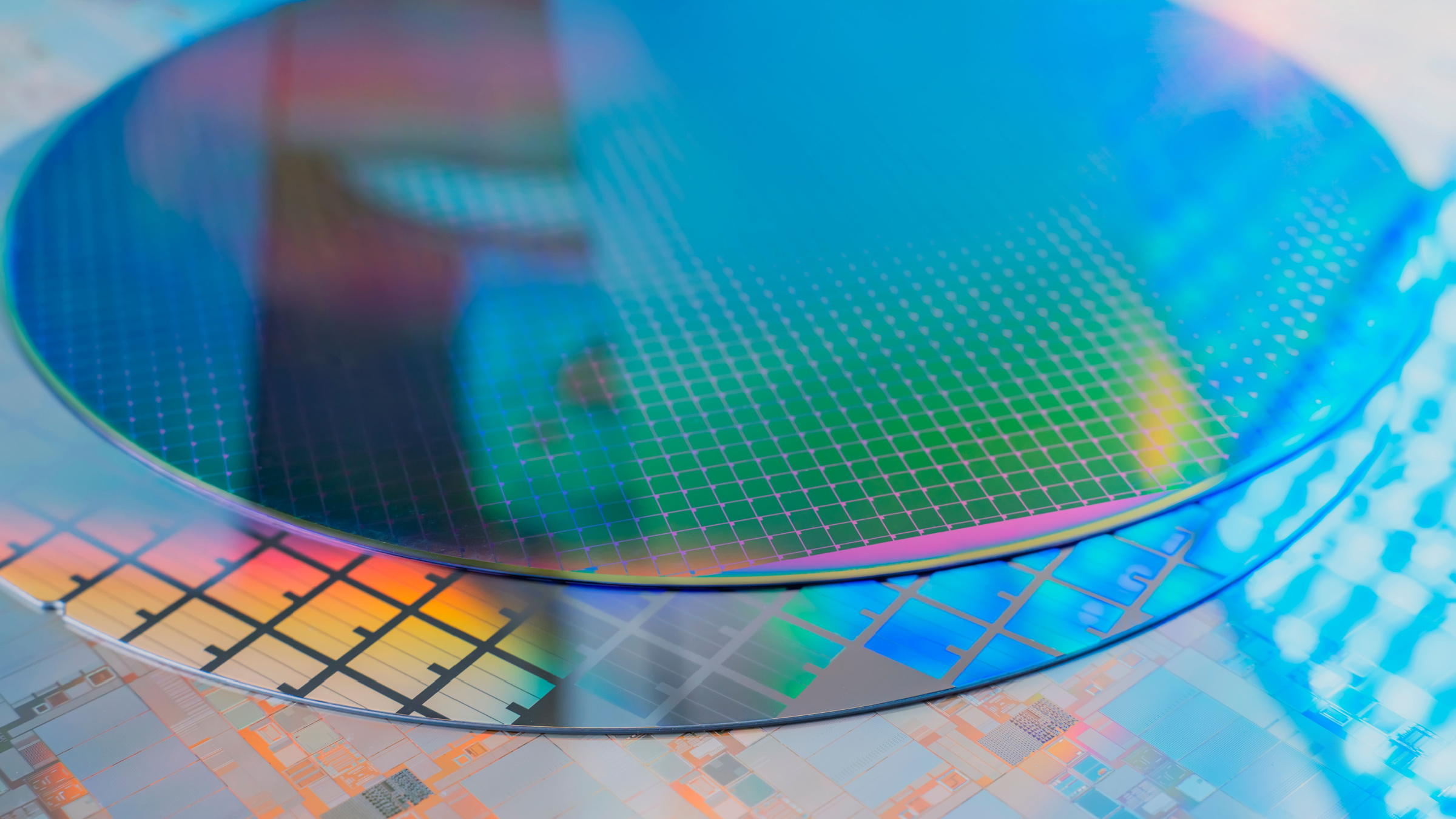
Semiconductor Manufacturing
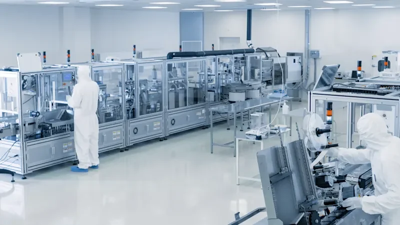
At Machinelab Solutions, we deliver precision robotics, machine vision, and AI-powered automation systems tailored to the extreme demands of semiconductor manufacturing. In an industry where nanometer-scale defects, ultra-clean environments, and relentless yield optimization define success, our integrated solutions provide the accuracy, speed, and intelligence required to enhance front-end and back-end processes while minimizing contamination risks and maximizing throughput.
Meeting the Challenges of Advanced Node Production
Semiconductor fabs operate at the limits of physics—shrinking geometries (sub-3nm nodes), complex 3D architectures (GAA, CFET), heterogeneous integration, and high-mix/low-volume runs for advanced packaging demand inspection and handling systems that are both ultra-precise and highly adaptable. Our solutions address critical pain points:
Detecting sub-micron defects invisible to traditional rule-based vision
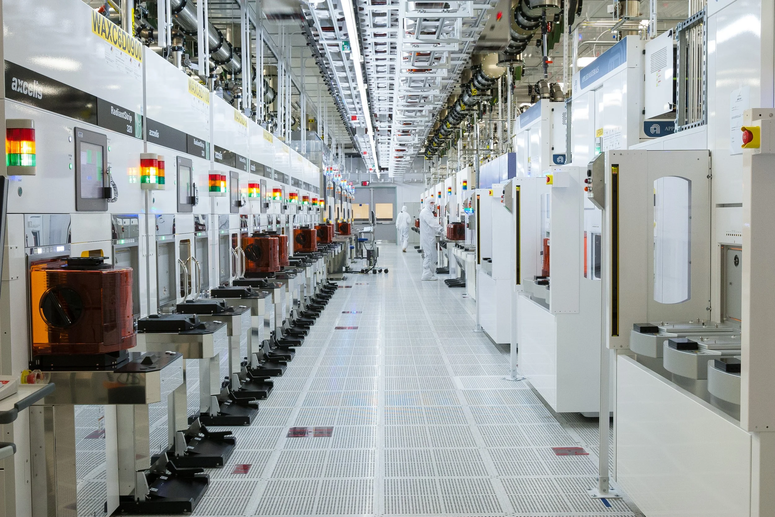
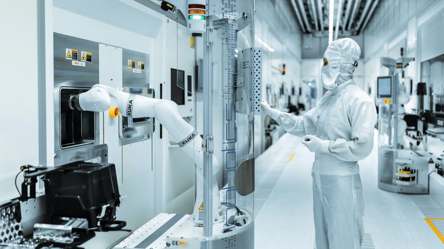
Enabling particle-free, non-contact robotic wafer handling in ISO Class 1 cleanrooms
Providing real-time, inline metrology and process verification
Supporting adaptive models that evolve with new process recipes and materials
Integrating seamlessly with existing fab automation, AMHS, and MES systems
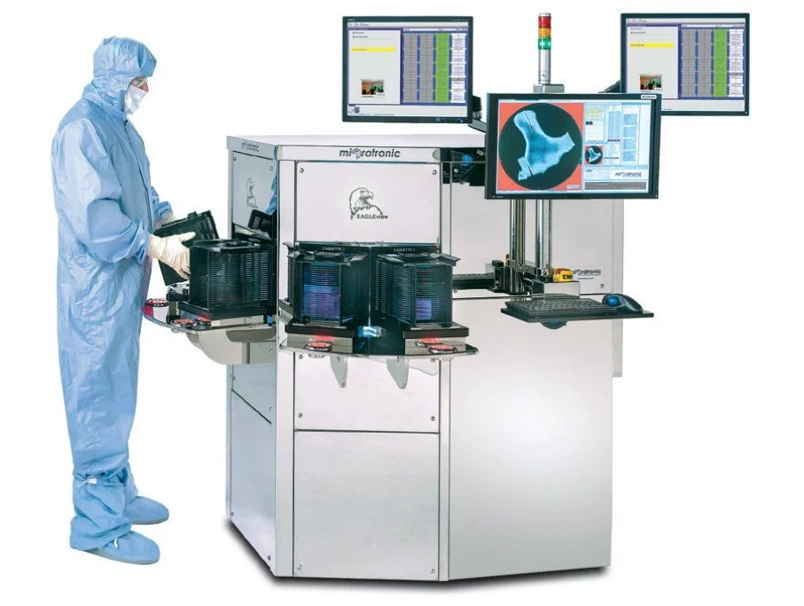
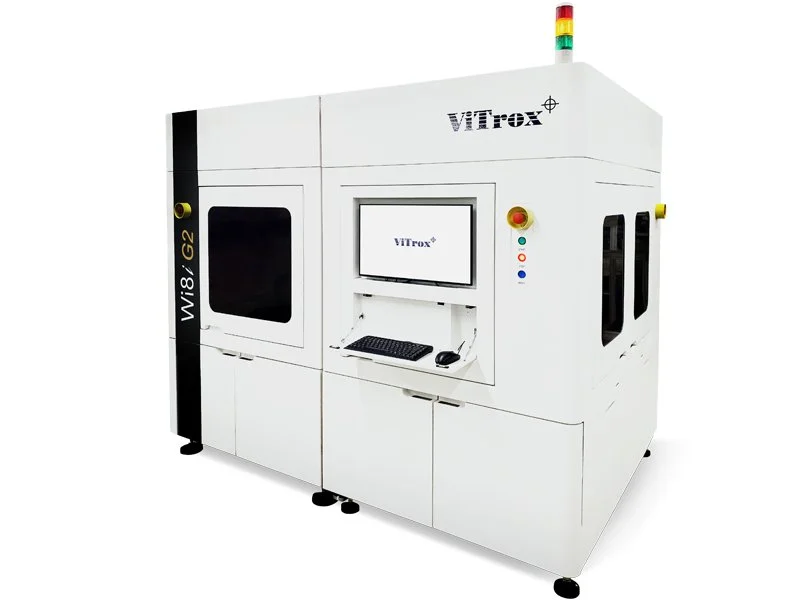
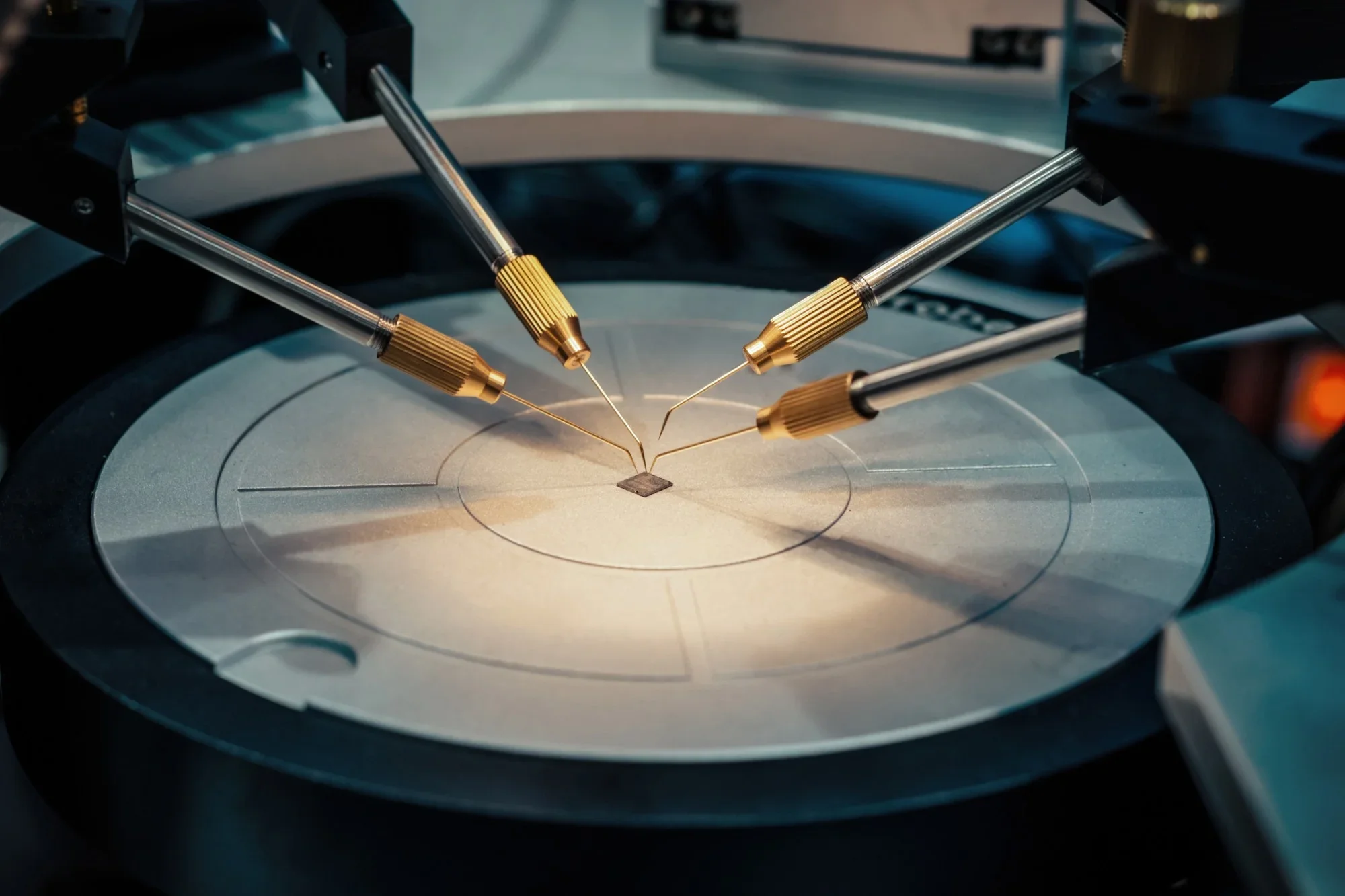
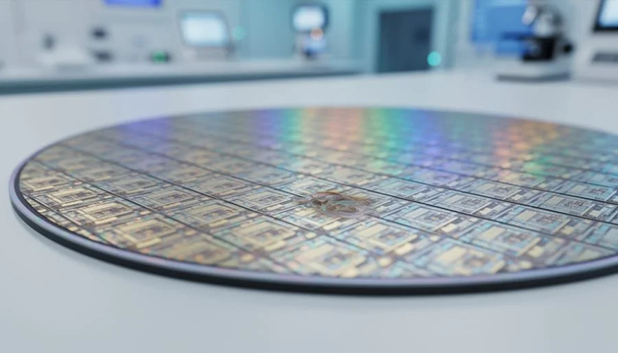
Wafer Defect Inspection & Classification — Powered by Cognex ViDi™ deep learning and MVTec HALCON hybrid AI models. Achieve >99% defect capture rate with near-zero false positives for scratches, particles, pattern anomalies, overlay errors, and contamination—deployed on high-resolution line-scan or area-scan cameras at production speeds.
Edge AI Real-Time Processing — NVIDIA Jetson Orin or Thor platforms with TensorRT-optimized inference deliver sub-10 ms latency for inline decisions. Multimodal analysis (vision + metadata) enables predictive classification and autonomous recipe adjustments without cloud dependency.
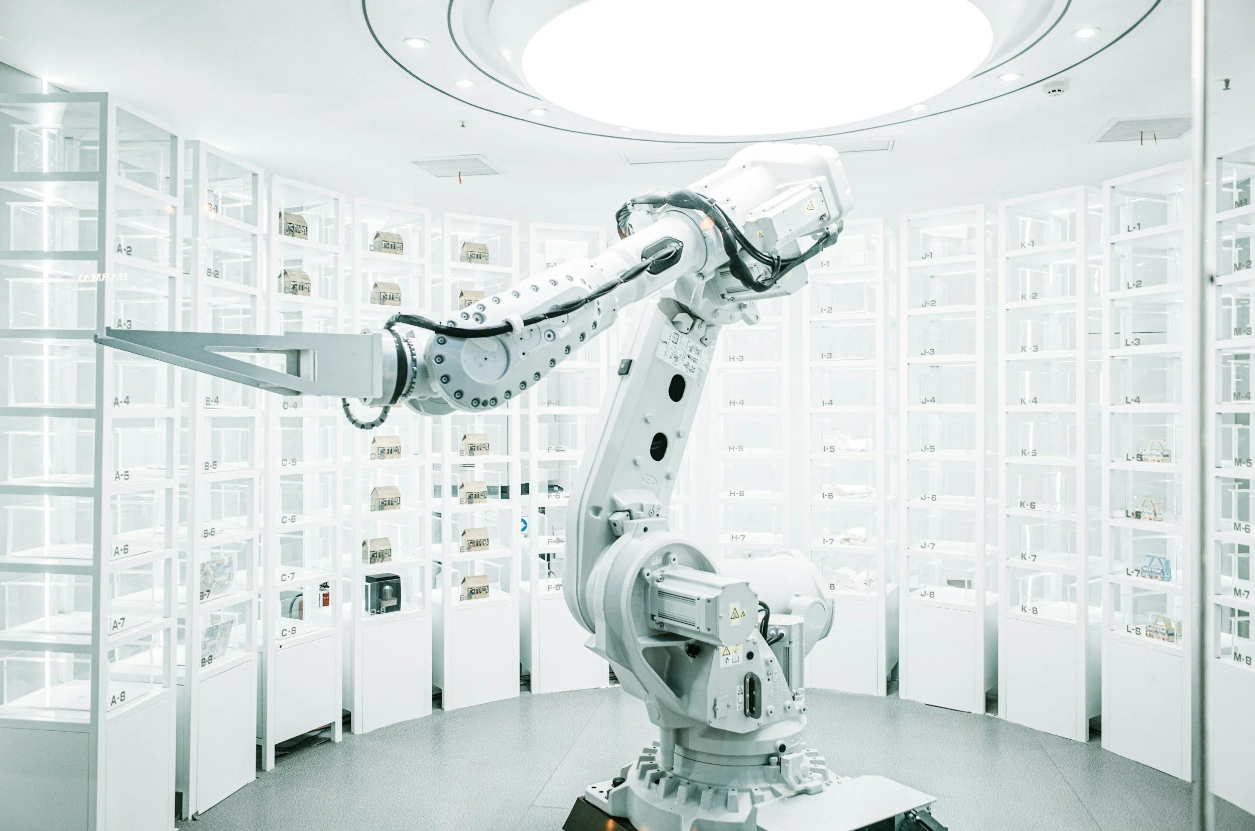
Cleanroom-Compatible Robotic Handling & Guidance — Precision 6-axis robots and collaborative cobots (cleanroom-rated) for wafer transfer, FOUP loading/unloading, and tool-to-tool transport. 3D vision-guided positioning ensures ±0.05 mm repeatability while maintaining particle generation within ISO Class thresholds.
Inline Metrology & Process Control — High-precision 3D vision for critical dimension (CD), overlay, film thickness, and bump height measurement. Data feeds directly into digital twin environments (Siemens + NVIDIA Omniverse) for real-time simulation, root-cause analysis, and predictive yield optimization.

Proven Value in Semiconductor Environments
Reduce scrap and rework by identifying killer defects early in the process
Increase effective equipment utilization (OEE) through faster, more accurate inspections
Minimize yield excursions with adaptive AI that learns from production data
Ensure traceability and compliance with automated, audit-ready visual records
Scale from R&D pilot lines to high-volume 300 mm fabs with modular, future-proof designs
We partner with leading technology providers—Cognex, MVTec, NVIDIA, Siemens, Basler, and cleanroom robotics specialists—to integrate best-in-class components into turnkey solutions. Whether enhancing an existing inspection station, automating wafer handling, or building a complete vision-guided process cell, our team manages full project lifecycle: design, integration, validation in cleanroom conditions, and ongoing support.
Contact Machinelab Solutions to discuss your requirements and discover how our expertise can elevate your semiconductor operations.
Request a consultation | Schedule a demonstration